
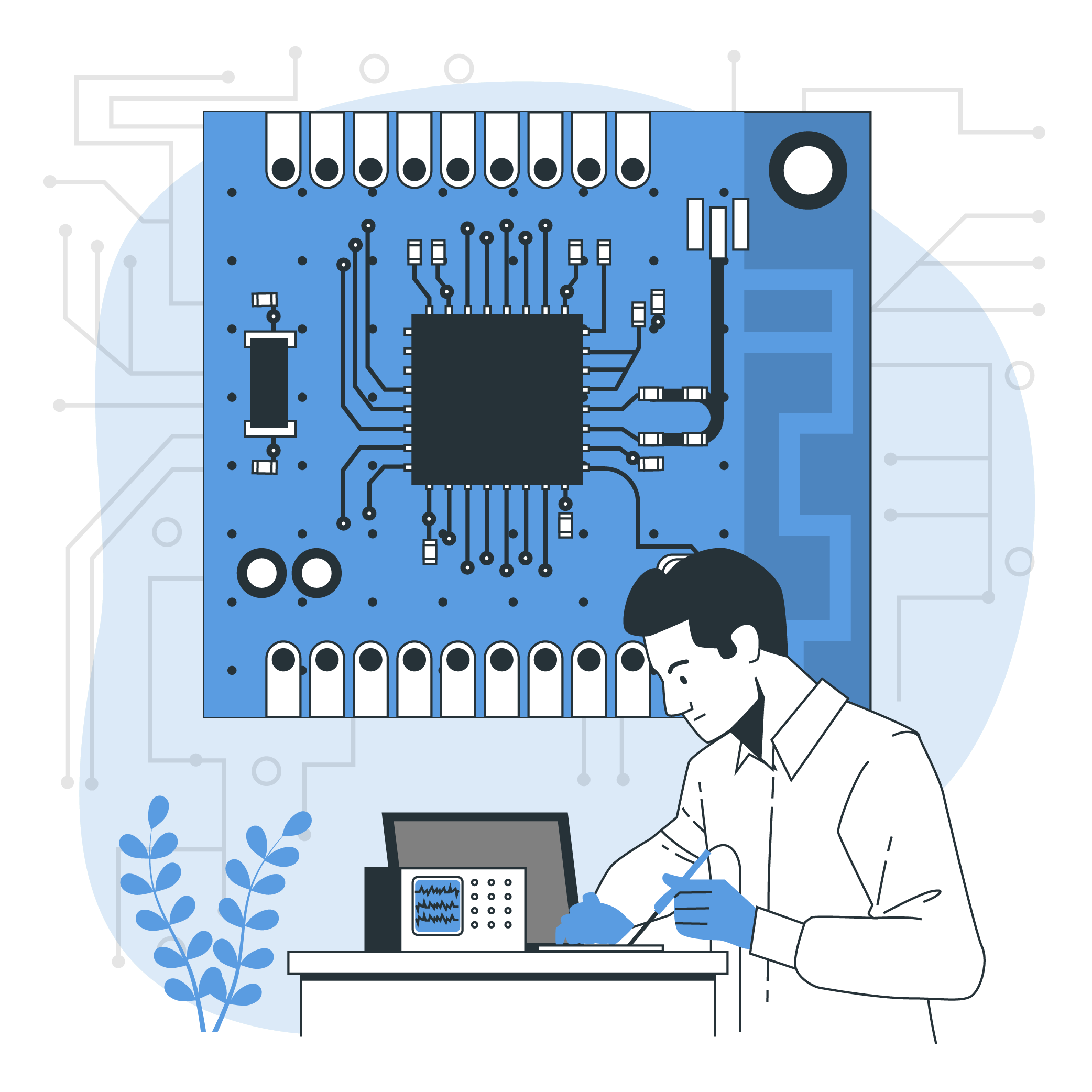
Electrical & Electronic Engineering
We offer high-precision electrical and electronic design services that support your products from schematic development to fully manufactured PCBs. Our electrical engineers work on complex analog/digital designs, power circuits, sensor interfaces, and more.


Work Process
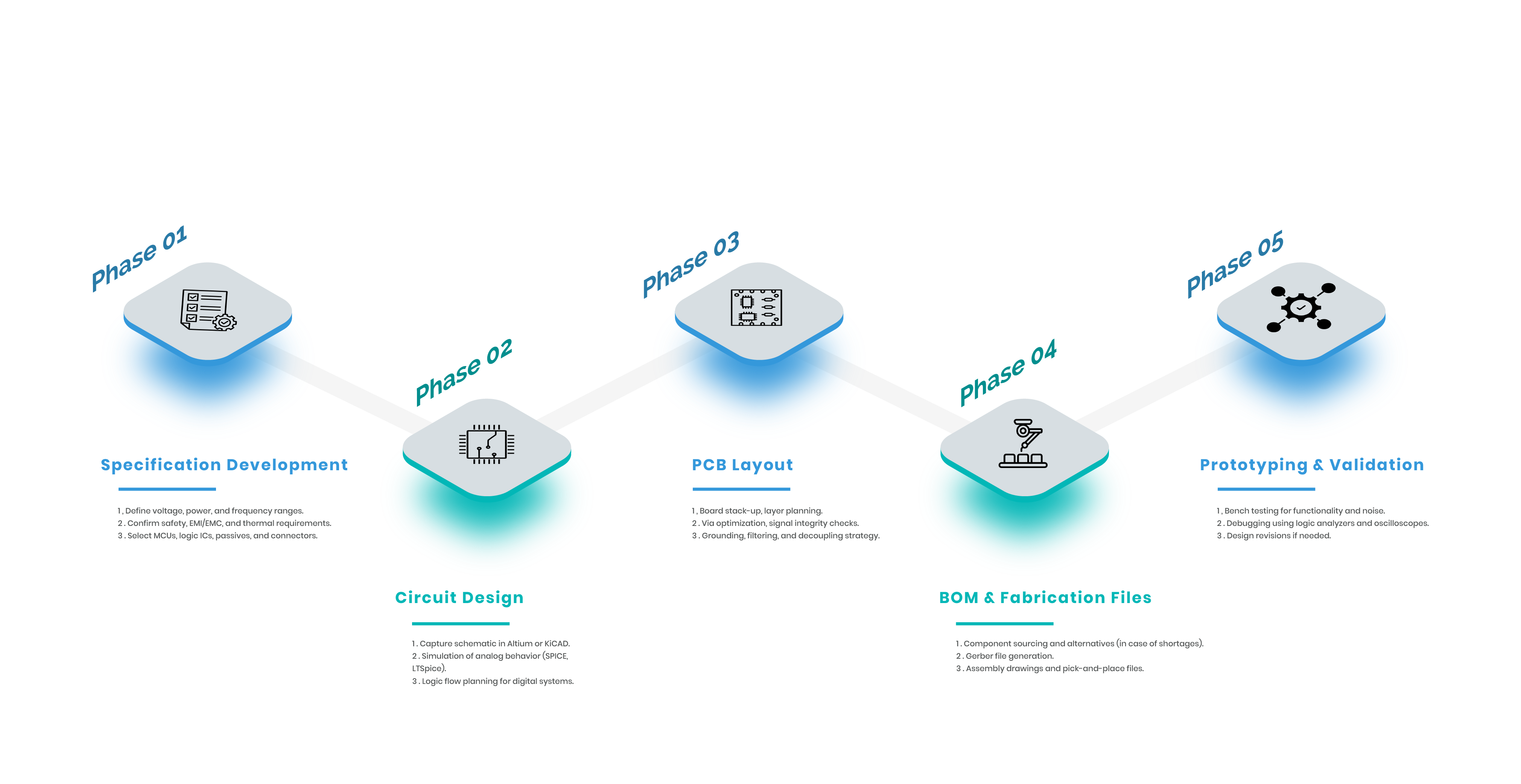
Phase 1: Specification Development
• Define voltage, power, and frequency ranges
• Confirm safety, EMI/EMC, and thermal
requirements
• Select MCUs, logic ICs, passives, and connectors
Phase 2: Circuit Design
• Capture schematic in Altium or KiCAD
• Simulation of analog behavior (SPICE,
LTSpice)
• Logic flow planning for digital systems
Phase 3: PCB Layout
• Board stack-up, layer planning
• Via optimization, signal integrity checks
• Grounding, filtering, and decoupling strategy
Phase 4: BOM & Fabrication Files
• Component sourcing and alternatives
• Gerber file generation
• Assembly drawings and pick-and-place files
Phase 5: Prototyping & Validation
• Bench testing for functionality and noise
• Debugging using logic analyzers and
oscilloscopes
• Design revisions if needed
Tools Used


.png)
Industries Served


Visual Suggestions
• PCB 3D renders
• Screenshot of multi-layer routing
• Bench test images with instruments
• Client submits initial sketches, references, and
intended product function.
• Our team studies dimensional constraints, load
requirements, and aesthetics.
• Create multiple low-fidelity concepts.
• 3D block models for volume and proportion.
• Internal component space planning.
• Create parametric models with SolidWorks or Fusion
360.
• Assembly models with motion simulation.
• Collision detection and kinematic chain simulation.
• FEA for stress, deformation, and thermal loads.
• Material selection for weight, strength, and cost.
• Iterative optimization using design of experiments
(DOE).
• 2D drawings for CNC/3D printing/injection molding.
• File formats: STL, STEP, IGES, DWG, PDF.
• Full documentation with exploded views and bill of
materials (BOM).